

Characterization of Unintentional Doping in Localized Epitaxial GaN Layers on Si Wafers by Scanning Spreading Resistance Microscopy|硅晶圆上局部外延氮化镓层中非故意掺杂的扫描扩展电阻显微镜表征
Thomas Kaltsounis, Helge Haas, Matthieu Lafossas, Simona Torrengo, Vishwajeet Maurya, Julien Buckley, Denis Mariolle, Marc Veillerot, Alain Gueugnot, Laurent Mendizabal, Yvon Cordier, and Matthew Charles
Abstract
This study investigates the unintentional doping introduced during the localized epitaxial growth of GaN on 200 mm silicon wafers. Three mask materials—SiN, SiO₂, and Al₂O₃—are compared to determine their influence on the electrical properties of the resulting GaN layers. Scanning Spreading Resistance Microscopy (SSRM) is used to spatially characterize the local resistance and carrier distribution, while Secondary Ion Mass Spectrometry (SIMS) is employed to verify the impurity concentrations. The results show that SiN and SiO₂ masks introduce high levels of unintentional doping, whereas an Al₂O₃ mask enables the growth of highly resistive GaN with carrier concentrations below 1 × 10¹⁶ cm⁻³. The researchers also obtain crack-free GaN structures with thicknesses approaching 7 μm, demonstrating progress toward GaN-on-Si material suitable for high-voltage vertical power devices.
Summary of the Paper
1. Research Objective
The study aims to determine how different mask materials influence unintentional doping during the localized Metal–Organic Vapor Phase Epitaxy (MOVPE) of GaN on silicon.
The main technological target is a thick, lightly doped GaN drift layer suitable for vertical power devices operating at approximately 1200 V. Such devices require a GaN layer with a carrier concentration around or below 1 × 10¹⁶ cm⁻³, while maintaining sufficient thickness and structural integrity.
The study also examines whether SSRM can reliably characterize very lightly doped GaN layers at concentration levels close to 10¹⁶ cm⁻³.
2. Methodology & Experimental Setup
Epitaxial growth: GaN structures were grown by MOVPE on 200 mm-diameter Si wafers containing AlN/AlGaN buffer layers, an undoped GaN layer, and an n-GaN template layer.
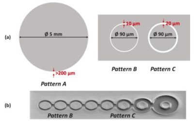
Mask comparison: Three 50 nm-thick mask materials—SiN, SiO₂, and Al₂O₃—were deposited and patterned before localized GaN growth. Six samples representing two epitaxial structures and the three mask materials were investigated.
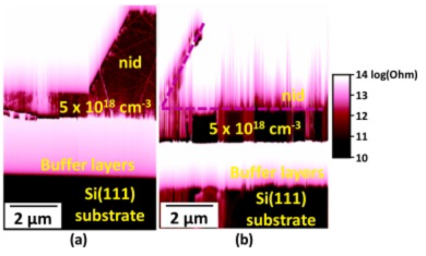
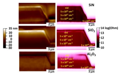
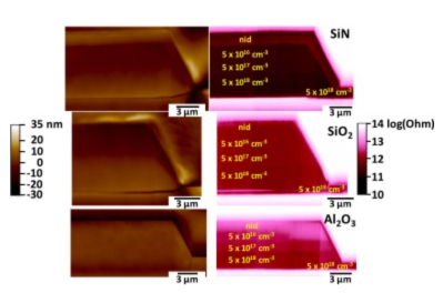
Calibration structure: One set of samples contained GaN layers with nominal Si-doping concentrations of 5 × 10¹⁸ cm⁻³, 5 × 10¹⁷ cm⁻³, and 5 × 10¹⁶ cm⁻³, together with a nominally undoped layer. These layers served as internal references for interpreting the SSRM response.
SSRM characterization: Top-view and cross-sectional SSRM measurements were performed using a Bruker Dimension ICON AFM equipped with doped-diamond-coated conductive probes. The technique measured local spreading resistance, which is related to the local resistivity and carrier concentration of the GaN.
Measurement conditions: Depending on the sample and measurement geometry, DC sample biases of −2 V, −6 V, or −8 V were applied between the conductive probe and the back contact.
Independent verification: SIMS measurements were used to determine the concentrations of silicon, oxygen, and carbon and to verify the trends observed through SSRM.
3. Key Findings
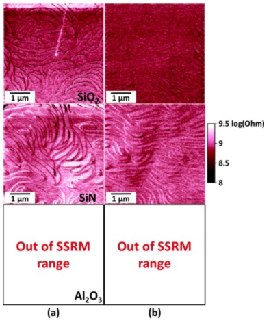
Strong mask-dependent doping: GaN grown using SiN and SiO₂ masks exhibited high unintentional doping. In several regions, the carrier or impurity concentration was on the order of 10¹⁸ cm⁻³, which is too high for the drift region of high-voltage vertical GaN devices.
Superior performance of Al₂O₃: The Al₂O₃ mask produced much more resistive GaN. SSRM clearly distinguished the intentionally doped layers, while the nominally undoped layer exhibited extremely high resistance.
Record-low unintentional doping: SIMS measurements supported the SSRM results and showed a silicon concentration as low as approximately 5 × 10¹⁵ cm⁻³ in the nominally undoped GaN grown with the Al₂O₃ mask. The combined results indicate a carrier concentration below 1 × 10¹⁶ cm⁻³.
Extension of SSRM capability: According to the authors, this is the first demonstration that SSRM can image GaN layers with doping concentrations on the order of 10¹⁶ cm⁻³.
Progress toward vertical GaN devices: Crack-free localized GaN structures with thicknesses of approximately 6–7 μm were obtained. Although still below the approximately 10 μm target, the results represent an important step toward GaN-on-Si drift layers for 1200 V vertical power devices.
中文整理
该研究围绕硅基氮化镓(GaN-on-Si)垂直功率器件所需的低掺杂漂移层展开。研究人员在200 mm硅晶圆上进行GaN局部选择性外延,并比较SiN、SiO₂和Al₂O₃三种掩膜材料对GaN非故意掺杂的影响。
实验结果表明,使用SiN或SiO₂作为外延掩膜时,掩膜中的硅及相关杂质可能在Ga原子扩散和外延生长过程中进入GaN,使非故意掺杂浓度达到约10¹⁸ cm⁻³。这一掺杂水平会使漂移层电阻过低,难以满足高耐压垂直GaN功率器件的要求。
相比之下,Al₂O₃掩膜可以明显减少硅杂质的引入。SSRM测得相应GaN层具有很高的局部电阻,SIMS进一步确认其非故意掺杂浓度低于1 × 10¹⁶ cm⁻³,部分区域的硅浓度约为5 × 10¹⁵ cm⁻³。
研究还获得了厚度接近7 μm、表面无裂纹的GaN局部外延结构,为进一步制备约10 μm厚、适用于1200 V级垂直功率器件的漂移层提供了实验基础。
【SSRM在该研究中的核心用途】
二维局部电阻与掺杂分布成像
SSRM利用导电探针扫描GaN表面或截面,测量探针下方的局部扩展电阻。由于扩展电阻与材料的局部电阻率及载流子浓度密切相关,因此研究人员可以直观比较不同外延层及不同位置的掺杂差异。
比较三种掩膜材料的污染效应
通过对SiN、SiO₂和Al₂O₃样品进行相同条件下的SSRM测量,研究人员发现,SiN和SiO₂样品边缘及外延层中的电阻明显偏低,说明存在较强的非故意掺杂;而Al₂O₃样品则表现出更高的电阻和清晰的层间差异。
分析外延层内部的纵向掺杂结构
截面SSRM能够同时显示不同深度的GaN层。研究人员利用已知掺杂浓度的GaN层作为内部校准参考,判断名义未掺杂层的电阻和载流子浓度,并观察掺杂随外延层深度的变化。
验证低掺杂GaN的可测量性
研究首次将SSRM应用于掺杂浓度约为10¹⁶ cm⁻³的GaN层成像,扩展了该技术在高阻宽禁带半导体中的实际测量范围。
与SIMS形成互补验证
SSRM提供高空间分辨率的局部电学分布信息,而SIMS提供Si、O和C等元素的浓度深度信息。两者结合,可以把“局部导电性变化”与“杂质来源”联系起来,提高对外延工艺问题的判断可靠性。
【技术贡献与价值】
为GaN外延工艺筛选提供直接依据
研究证明,Al₂O₃比SiN和SiO₂更适合作为低掺杂GaN局部外延的掩膜材料。这一结论可以直接指导垂直GaN功率器件的材料和工艺开发。
建立工艺、掺杂分布与器件性能之间的联系
漂移层的掺杂浓度直接影响功率器件的耐压、漏电和导通电阻。SSRM能够在器件制造前定位异常导电区域,使外延质量评估不再局限于大面积平均测量。
推动SSRM向宽禁带半导体低掺杂分析扩展
GaN表面氧化层、接触特性和高电阻都会增加SSRM的测量难度。本研究通过掺杂参考层、导电金刚石探针和SIMS交叉验证,证明SSRM能够用于10¹⁶ cm⁻³量级的GaN掺杂分析。
支持高压垂直GaN-on-Si器件开发
低于1 × 10¹⁶ cm⁻³的载流子浓度和约7 μm的无裂纹GaN结构,说明局部外延路线已接近1200 V级垂直器件所需的厚漂移层和低掺杂要求。
【测量局限】
SSRM信号不仅受到载流子浓度影响,也会受到探针接触面积、表面形貌、氧化层及截面抛光损伤的影响。因此,该研究中的SSRM绝对定量能力仍有限,部分结果需要依靠已知掺杂层进行校准,并通过SIMS加以验证。它的突出优势主要在于高空间分辨率的二维电学成像和不同样品之间的相对比较。
原文链接:

