Indepth doping assessment of thick doped GaAs layer by scanning spreading resistance microscopy
Lanpeng Qiang, Emmanuel Chereau, Philippe Regreny, Geoffrey Avit, Agnès Trassoudaine, Evelyne Gil, Yamina André, Jean-Marie Bluet, David Albertini, Georges Brémond
Abstract
Scanning spreading resistance microscopy (SSRM) measurements were performed on GaAs thick films grown by hydride vapor phase epitaxy technology under different growth conditions to evaluate their carrier concentrations. For this purpose, a calibration curve was established based on a multilayer staircase structure grown by molecular beam epitaxy. The dopant calibration range measured by secondary ion mass spectrometry is from 5 × 10¹⁶ to 1019 cm−3. An abnormal phenomenon in the calibration process was explained by taking into account the parasitic parallel resistance of the calibration samples. Finally, the calibration curve was used to quantitatively analyze the carriers inside the Zn doping p-type GaAs film from 4 × 10¹⁶ to 1018 cm−3 range. We demonstrate here the applicability of SSRM to the in-depth analysis of thick epilayers, providing new inputs for the control of thick film technologies.
Summary of the paper
This paper explores the application of scanning spreading resistance microscopy (SSRM) for quantitative in-depth doping assessment of thick GaAs layers grown via hydride vapor phase epitaxy (HVPE).
Key steps and findings include:
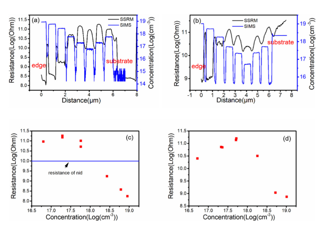
A calibration curve was established using MBE-grown GaAs multilayer staircase structures (Be-doped p-type, Si-doped n-type), with dopant concentrations validated by secondary ion mass spectrometry (SIMS) ranging from 5×10¹⁶ to 1019 cm−3; anomalies in calibration (e.g., resistance increase with carrier concentration in low-doped regions) were explained by parasitic parallel resistance.
SSRM was applied to cross-sections of Zn-doped p-type HVPE GaAs films, enabling quantitative carrier concentration analysis (ranging from 4 × 10¹⁶ to 1018 cm−3) and revealing that doping concentration rises with diethylzinc (DEZ) flow rate while remaining uniform across the film (slight edge increase only).
The study demonstrates SSRM's efficacy for characterizing thick GaAs epilayers, offering valuable insights for optimizing HVPE-based thick film technologies in applications like solar cells and quasisubstrates.

在本篇文章中,扫描扩展电阻显微镜SSRM具体的应用场景和作用如下:
- 建立定量校准体系:以分子束外延(MBE)生长的 GaAs 多层阶梯结构为校准样品(p 型为 Be 掺杂,n 型为 Si 掺杂),结合二次离子质谱(SIMS)测得的掺杂浓度(p 型:6×10¹⁶-9×10¹⁸ cm⁻³;n 型:5×10¹⁶-10¹⁹ cm⁻³),通过 SSRM 表征不同掺杂层的电阻值,构建电阻与载流子浓度的校准曲线(p 型曲线斜率 - 1.99、截距 43.8;n 型曲线斜率 - 1.74、截距 41.1),同时引入寄生并联电阻解释校准中 “低掺杂区电阻随载流子浓度升高而增大” 的异常现象,为后续定量分析奠定基础。
- 厚 GaAs 膜载流子浓度定量分析:对氢化物气相外延(HVPE)生长的 Zn 掺杂 p 型 GaAs 厚膜进行横截面 SSRM 表征(采用 Dimension Icon 显微镜,搭配镀高掺杂导电金刚石涂层的 Si 探针,施加正向偏压),结合已建立的校准曲线,确定厚膜中不同区域的载流子浓度 —— 如衬底载流子浓度约 5.4×10¹⁶ cm⁻³,掺杂层载流子浓度约 2.1×10¹⁸ cm⁻³,且明确载流子浓度随二乙基锌(DEZ)流量增加而升高,同时验证掺杂层内浓度整体均匀、仅边缘略增的分布特征。
- 非有意掺杂(nid)区载流子扩散评估:利用 SSRM 表征校准样品的 nid 区电阻(p 型 nid 区电阻 1.6×10¹⁰-3.2×10¹⁰ Ω,n 型 nid 区电阻 1.6×10¹¹-5.0×10¹¹ Ω),结合校准曲线外推,定量得出 nid 区因载流子扩散产生的载流子浓度(p 型:5.4×10¹⁶-7.7×10¹⁶ cm⁻³;n 型:7.9×10¹⁶-1.5×10¹⁷ cm⁻³),补充了载流子迁移对浓度分布影响的分析。


